 Kyunghyun Lee
2024.12.18
Kyunghyun Lee
2024.12.18
AI-Powered PCB Design Automation
Printed circuit boards (PCBs) are an integral module that is part of every electronic device in existence. From KRW 1,000 toys to mobile phones, computers, and appliances like refrigerators, they are an integral part of our everyday lives. A PCB is a thin plate that contains the circuitry for the operation of electronic components.
The PCB contains a processor that performs calculations, passive circuit components such as resistors and capacitors, and a regulator that provides the power required for these components. They are electrically connected using copper wires, following a planned circuit diagram to ensure proper functionality. The image to the left of Image 1 is a common example of a PCB, where the lines running through the board are copper wires that carry signals. Without this PCB technology, all components would have to be connected directly with copper wires, as shown in the picture to the right, and mass production that we have today would not be possible.
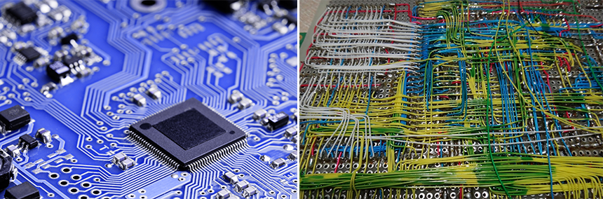
Image 1. Example of a printed circuit board (PCB) (left), circuit consisting of jumper cables (right)[1]
So, how are these PCBs designed? Every PCB is designed with an intended purpose. For example, a PCB in a fan has a clearly defined task that the PCB needs to accomplish, such as controlling a motor at the desired speed. Once the board's mission is determined, the different components needed to accomplish that task are selected and a schematic, a design diagram of how the components should be connected, is created. The schematic must take into account all the details, such as how the components will communicate with each other and how they will be powered. Then comes the component placement step, in which it is determined where and in what direction the components will be placed on the board, considering their shape and which components they need to connect to. Once the components are placed, the PCB is completed by the circuit wiring step, which actually uses copper wires to connect the components as designed in the schematic.
LG Electronics, LG Display, LG Innotek, and other LG affiliates perform thousands of PCB design tasks of various kinds every year, each requiring anywhere from a few hours to more than a dozen days of work. PCB auto-routing aims to enable AI to assist experts in efficiently completing complex circuit routing in a short period of time.
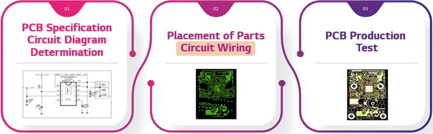
Image 2. PCB design process
PCB wiring problems have several characteristics that make them different from traditional pathfinding problems. First of all, there are several constraints on the wiring process. Different signal wires must be separated from each other by a certain distance to avoid short circuits, each signal wire has a different thickness depending on the amount of current required, and there are areas depending on the board where wiring is prohibited.
The second characteristic is that each wire may have to follow a deliberately inefficient path in order to take into account other wires. Although wiring along the shortest path is electrically beneficial, signal wires may sometimes intentionally take longer routes to ensure they connect properly within a limited space.
The final characteristic is that it is a multilayer design that uses multiple layers. A PCB basically utilizes 2 layers, a front and back, to mount components, and the wiring also uses these 2 layers, but additional layers can be added inside depending on the amount of space or current required. When several signals need to fit into a limited amount of space, such as in a cell phone, we sometimes use 8 or 12 layers. Signal lines can traverse multiple layers using VIAs, which connect signals between layers. In this case, VIAs typically take up more space than signals and should be used with caution.
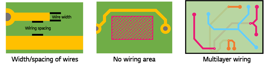
Image 3. Characteristics of PCB design problems
As such, PCB problems have many characteristics that cannot be solved by a simple pathfinding problem. LG AI Research approaches this problem using both grid-based and continuous space-based methods. In the case of the grid-based method, the PCB board is divided into regular intervals for exploration, and it is approached by converting it into a Steiner Tree Packing Problem (STPP) in the field of combinatorial optimization. The continuous space-based method solves the problem by utilizing the board as it is without this conversion.
The two methods have clear advantages and disadvantages and are complementary to each other. The grid-based method uses a grid to speed up the exploration, but the process of converting to a grid has the disadvantage of causing thatch and violating constraints. On the other hand, the continuous space method is able to satisfy constraints exactly but has the disadvantage of being slow because constraint checks are performed every time during the exploration process.
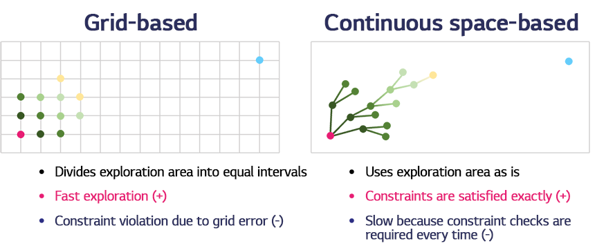
Image 4. Advantages and disadvantages of grid-based algorithms and continuous space-based algorithms
At LG AI Research, we first explore the connection methods that satisfy the majority of constraints by performing a grid-based exploration method and then use this as a guide to narrow the exploration area to accelerate the exploration in continuous space while exploring solutions that accurately satisfy the constraints. In this process, we have developed and are utilizing the Pathfinder+ algorithm, which detects areas that violate constraints and penalizes the collision areas for re-exploration. This process of updating the cost is performed iteratively to ensure that each signal satisfies all constraints. This process results in a solution that satisfies the constraints on the grid.
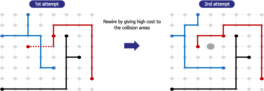
Image 5. Pathfinder+ collision solving
However, even if you derive the correct solution on the grid, restoring it to the original PCB problem may introduce constraint violations due to grid errors. To solve this problem, the solution is explored in continuous space. Continuous space exploration utilizes the rapid-exploring random tree (RRT) algorithm, one of the pathfinding algorithms, modified for PCB problems (RRT-PCB), and to accelerate exploration, we developed a method to increase sampling efficiency by utilizing the solutions explored on the grid.
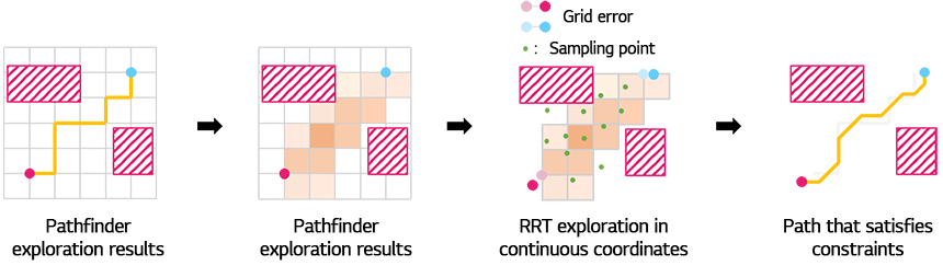
Image 6. RRT-PCB exploration using Pathfinder+ guide
So far, The research to tackle the automated routing of PCBs conducted by LG AI Research was introduced. It has been verified through various actual products of LG affiliates and confirmed that it can perform wiring that reflects various constraints. However, there are still areas that need to be improved before the wiring results can be directly utilized in actual products. In particular, in the case of actual PCBs used in the industry, there are various recommendations that are difficult to define clearly, and they are implemented on the PCB through the experience of engineers.
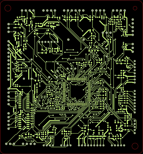
Image 7. Part of a PCB designed automatically by AI
To solve these problems, LG AI Research is conducting research to train from existing engineers' wiring data to produce results similar to actual designs. Through this, we expect to be able to effectively capture the expertise of advanced engineers and reflect it into PCB design automation.
▶ Evolving AI in industry - AI-Powered PCB Design Automation
- 참고
- [1] http://m.todaysppc.com/renewal/view.php?id=free&no=212919